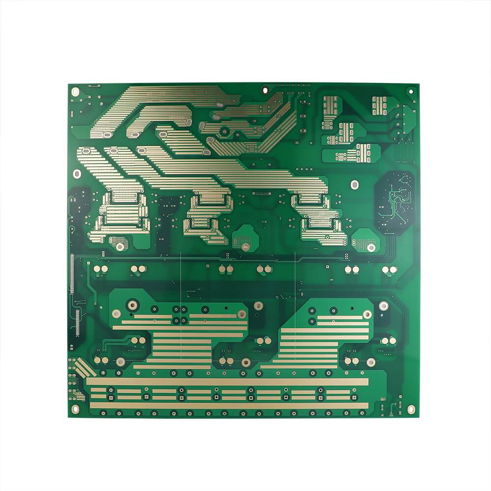
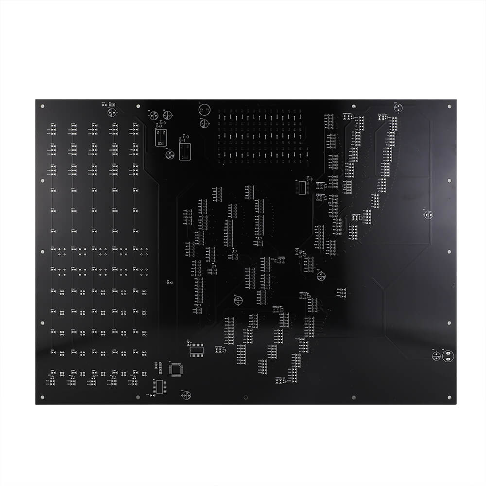
As electronic devices become more complex and compact, the demand for high-density multilayer printed circuit boards (PCBs) has surged. Hongmy, a leading PCB manufacturer, specializes in producing high-quality multilayer PCBs that deliver superior performance for a variety of applications. This article explores the benefits of high-density multilayer PCBs, their main applications, and essential manufacturing tips to ensure optimal quality and functionality.
What Are High-Density Multilayer PCBs?
High-density multilayer PCBs consist of multiple layers of circuitry stacked within a compact form factor, allowing for complex electrical connections and efficient use of space. This dense configuration supports sophisticated electronic applications, offering higher circuit density and improved performance over traditional single- or double-layer PCBs.

Benefits of High-Density Multilayer PCBs
Enhanced Circuit DensityMultilayer PCBs allow manufacturers to incorporate more circuitry within a smaller area, enabling compact designs without compromising functionality. This high density is essential for advanced applications requiring intricate electrical pathways.
Improved Signal IntegrityWith multiple layers, high-density PCBs minimize signal loss and improve signal integrity by optimizing the routing of complex circuitry. The design reduces interference, maintaining clearer signals and better overall device performance.
Compact and Lightweight DesignThese PCBs are ideal for applications where space and weight are critical factors. By layering the circuits, designers can fit complex circuits into smaller devices, making them suitable for modern, portable electronics.
Greater ReliabilityMultilayer PCBs offer robust interconnections due to their intricate layering and use of high-quality materials, which enhance the reliability and longevity of the device. The additional layers provide built-in redundancies that ensure stable performance in various environments.
High-Performance CapabilitiesBy accommodating complex circuitry, high-density multilayer PCBs can support the high-speed and high-frequency requirements of advanced applications, such as telecommunications, medical equipment, and aerospace technology.
Applications of High-Density Multilayer PCBs
Due to their compact and efficient design, high-density multilayer PCBs are widely used across various industries:
- Consumer Electronics: Devices such as smartphones, tablets, and wearable tech rely on high-density multilayer PCBs for their compact size and performance requirements.
- Telecommunications: Network equipment, including routers and servers, uses these PCBs for reliable signal transmission and high data processing capabilities.
- Medical Devices: Complex medical equipment, including imaging systems and diagnostic devices, benefit from the compactness and reliability of multilayer PCBs.
- Automotive and Aerospace: These industries require durable, high-performance PCBs for applications like engine controls, navigation systems, and avionics.
- Industrial Equipment: Robotics and automation systems leverage high-density multilayer PCBs to enable efficient and precise control within compact designs.
Manufacturing Tips for High-Density Multilayer PCBs
Design for Manufacturability (DFM)Start with a DFM approach to ensure the design aligns with production capabilities. DFM reduces potential errors, ensuring that the high-density multilayer PCB is optimized for streamlined manufacturing, lowering costs and improving quality.
Quality Material SelectionUse high-quality materials with excellent heat resistance, low dielectric loss, and high glass transition temperatures (Tg). Materials like FR4 and polyimide are ideal for supporting the durability and signal integrity of multilayer PCBs.
Precision in Layer StackingEnsure precise alignment and stacking of the layers to avoid issues during the bonding and lamination stages. Accurate stacking is critical for achieving the desired functionality and durability of high-density PCBs.
Enhanced Inspection TechniquesImplement advanced inspection methods, such as X-ray or automated optical inspection (AOI), to identify any defects, misalignments, or inconsistencies in the PCB layers. Inspection ensures quality and functionality throughout production.
Thermal Management SolutionsSince high-density multilayer PCBs often operate in high-performance devices, managing heat dissipation is essential. Integrate effective thermal management solutions, such as heat sinks or conductive vias, to prevent overheating and maintain device longevity.
Testing and Quality ControlRigorously test each PCB to ensure it meets performance standards, especially for critical applications in telecommunications and medical devices. Functional testing, impedance control, and stress tests are valuable steps to ensure reliable end products.

Choosing Hongmy for High-Density Multilayer PCBs
At Hongmy, we specialize in manufacturing high-density multilayer PCBs that meet the demands of modern technology. Our commitment to precision, quality materials, and rigorous testing ensures that our PCBs deliver consistent performance across a wide range of applications. With our expertise and cutting-edge facilities, we provide tailored solutions for clients requiring reliable, high-quality PCBs for advanced electronics.
Conclusion
High-density multilayer PCBs offer unparalleled benefits in terms of compact design, high performance, and reliability, making them an ideal choice for advanced electronics across industries. Whether for consumer gadgets or aerospace equipment, these PCBs drive innovation in compact and complex designs. By choosing a trusted manufacturer like Hongmy, you can be confident in the performance and durability of your high-density multilayer PCBs. For more information, visit Hongmy's website to explore our offerings and see how we can support your next project.

