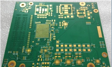
Building a multilayer PCB (Printed Circuit Board) is a complex but rewarding process that allows for compact, high-performance circuit designs. Unlike single-layer PCBs, multilayer boards consist of several layers of conductive material separated by insulating layers. This guide will walk you through the essential steps involved in creating a multilayer PCB, ensuring that you achieve a high-quality, functional circuit board.
1. Understand the Basics
Before diving into the design and manufacturing process, it’s important to understand what a multilayer PCB is. Multilayer PCBs are composed of multiple layers of circuitry and insulating material. They are used in applications where space is limited and complex circuits are required. Each layer in a multilayer PCB serves a specific function, such as signal routing or power distribution.

2. Define Your Requirements
Start by defining the requirements of your PCB. This includes:
- Circuit Complexity: Determine the number of layers needed based on the complexity of the circuit.
- Size and Shape: Define the physical dimensions and shape of your PCB.
- Electrical Specifications: Consider voltage, current, and signal integrity requirements.
- Material Selection: Choose appropriate materials for the layers, such as FR4, Rogers, or other high-frequency materials.
3. Design the PCB Layout
Use PCB design software to create your board layout. The design process includes:
- Schematic Design: Create a schematic diagram of your circuit to represent the connections between components.
- Layer Stack-Up: Define the stack-up of the PCB layers, including the arrangement of signal, power, and ground layers.
- Routing: Route the electrical connections between components, ensuring minimal interference and optimal signal integrity.
- Design Rules Check (DRC): Perform a design rules check to ensure that your layout meets manufacturing specifications.
4. Prepare the Design Files
Once the design is complete, prepare the necessary files for manufacturing. This typically includes:
- Gerber Files: Provide detailed information about the PCB layers, including copper traces, solder mask, and silkscreen layers.
- Bill of Materials (BOM): List all components required for the PCB assembly.
- Assembly Instructions: Include any specific instructions for the assembly process.
5. Select a Manufacturer
Choose a reliable PCB manufacturer, such as Hongmy Circuits, to produce your multilayer PCB. When selecting a manufacturer, consider:
- Experience: Ensure the manufacturer has experience in producing multilayer PCBs.
- Quality: Look for certifications and quality control measures to ensure high manufacturing standards.
- Capabilities: Verify that the manufacturer can handle the specific requirements of your PCB design.
6. Fabrication Process
The fabrication of a multilayer PCB involves several steps:
- Layer Preparation: Each layer of the PCB is created separately using processes like etching and lamination.
- Layer Alignment: Layers are aligned and bonded together using heat and pressure.
- Drilling: Holes for vias and component mounting are drilled through the board.
- Plating: The holes are plated with copper to establish electrical connections between layers.
- Finalization: The board is cut to size, and final features like solder mask and silkscreen are applied.
7. Testing and Quality Assurance
After fabrication, conduct thorough testing to ensure the PCB functions as intended. This includes:
- Electrical Testing: Verify that all connections are correct and that there are no short circuits or open circuits.
- Visual Inspection: Check for any physical defects or inconsistencies in the board.
8. Assembly
Once testing is complete, assemble the components onto the PCB. This involves:
- Soldering: Attach components to the board using soldering techniques, such as wave soldering or reflow soldering.
- Inspection: Perform a final inspection to ensure all components are properly mounted and soldered.
Conclusion
Building a multilayer PCB requires careful planning, precise design, and meticulous manufacturing processes. By following these steps and working with a reputable manufacturer like Hongmy Circuits, you can create a high-quality, reliable multilayer PCB that meets your technical and performance requirements. Whether you’re designing for consumer electronics, industrial applications, or advanced technologies, a well-built multilayer PCB is key to achieving optimal circuit performance.

