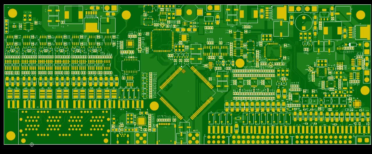
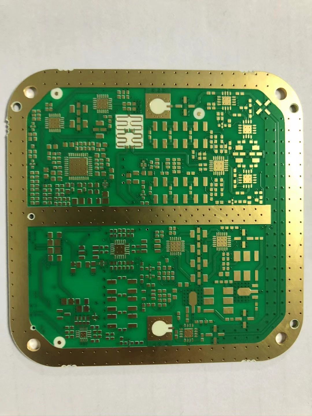
In the ever-evolving world of electronics, the need for efficient, high-performance printed circuit boards (PCBs) has never been greater. Among the various PCB designs, the 6-layer impedance circuit board PCB stands out as a crucial component in modern electronic devices. This article delves into the benefits of using a 6-layer impedance circuit board PCB, particularly in applications where signal integrity and performance are paramount.
What is a 6-Layer Impedance Circuit Board PCB?
A 6-layer impedance circuit board PCB is a type of multi-layer pcb that consists of six layers of conductive material separated by insulating layers. The term "impedance" refers to the resistance of the circuit to alternating current (AC) signals, which is crucial in maintaining signal integrity, especially in high-frequency applications.

Key Benefits of a 6-Layer Impedance Circuit Board PCB
1.Enhanced Signal Integrity
One of the primary benefits of a 6-layer impedance circuit board PCB is its ability to maintain signal integrity. In high-speed circuits, impedance control is vital to prevent signal loss, reflections, and interference. By carefully designing the PCB with controlled impedance, the 6-layer structure ensures that signals are transmitted with minimal distortion, which is essential for applications such as telecommunications, medical devices, and advanced computing systems.
2.Reduced Electromagnetic Interference (EMI)
Electromagnetic interference (EMI) can significantly degrade the performance of electronic devices. A 6-layer PCB design helps mitigate EMI by providing dedicated ground and power planes within the layers. These planes act as shields, reducing the amount of EMI that can affect the signal traces, thereby ensuring more reliable operation in environments with high electrical noise.
3.Increased Power Distribution Efficiency
The 6-layer PCB structure allows for better power distribution across the board. By incorporating dedicated power planes, the board can efficiently distribute power to various components, reducing voltage drops and ensuring stable operation. This is particularly important in complex circuits where multiple components require precise power delivery.
4.Compact and Space-Saving Design
As electronic devices become smaller and more compact, the demand for space-efficient PCB designs has increased. A 6-layer impedance circuit board PCB enables designers to pack more functionality into a smaller footprint without compromising performance. The multi-layer design allows for the integration of more components and signal routes within the same board area, making it ideal for compact electronic devices.
5.Improved Thermal Management
Heat dissipation is a critical factor in the reliability and longevity of electronic devices. The multi-layer structure of a 6-layer PCB provides better thermal management by allowing heat to spread across multiple layers, reducing the risk of hotspots. Additionally, the use of thermal vias—holes that connect the layers—helps transfer heat away from critical components, ensuring stable operation even in high-power applications.
6.Greater Design Flexibility
The 6-layer PCB design offers greater flexibility for engineers in terms of routing and layer stack-up. This flexibility allows for more complex circuits to be implemented without the need for multiple boards, reducing overall system complexity and cost. Additionally, the ability to control impedance across different layers provides more options for optimizing signal paths and reducing crosstalk between traces.
7.Cost-Effective Manufacturing
While the initial design and prototyping of a 6-layer PCB may be more expensive than simpler designs, the benefits in terms of performance, reliability, and space savings often outweigh the costs. Moreover, advancements in PCB manufacturing technologies have made it possible to produce multi-layer PCBs at a competitive cost, making them an attractive option for a wide range of applications.

Applications of 6-Layer Impedance Circuit Board PCBs
6-layer impedance circuit board PCBs are widely used in various high-performance applications, including:
Telecommunications Equipment: Ensuring signal integrity and reducing EMI in communication devices.
Medical Devices: Providing reliable and compact solutions for advanced medical equipment.
Consumer Electronics: Enabling the design of compact, high-performance devices such as smartphones and tablets.
Automotive Electronics: Supporting the development of advanced driver-assistance systems (ADAS) and in-vehicle infotainment systems.
Conclusion
The 6-layer impedance circuit board PCB is a powerful tool in the hands of modern electronics designers. Its ability to enhance signal integrity, reduce EMI, and improve power distribution makes it an essential component in a wide range of high-performance applications. As technology continues to advance, the demand for sophisticated PCB designs like the 6-layer impedance circuit board will only grow, driving innovation and enabling the development of the next generation of electronic devices.
For more information on 6-layer impedance circuit board PCBs and to explore high-quality products, visit HongMy Circuits. Their expertise in PCB manufacturing ensures that you receive top-tier products tailored to your specific needs.

