Understanding Multilayer PCBs
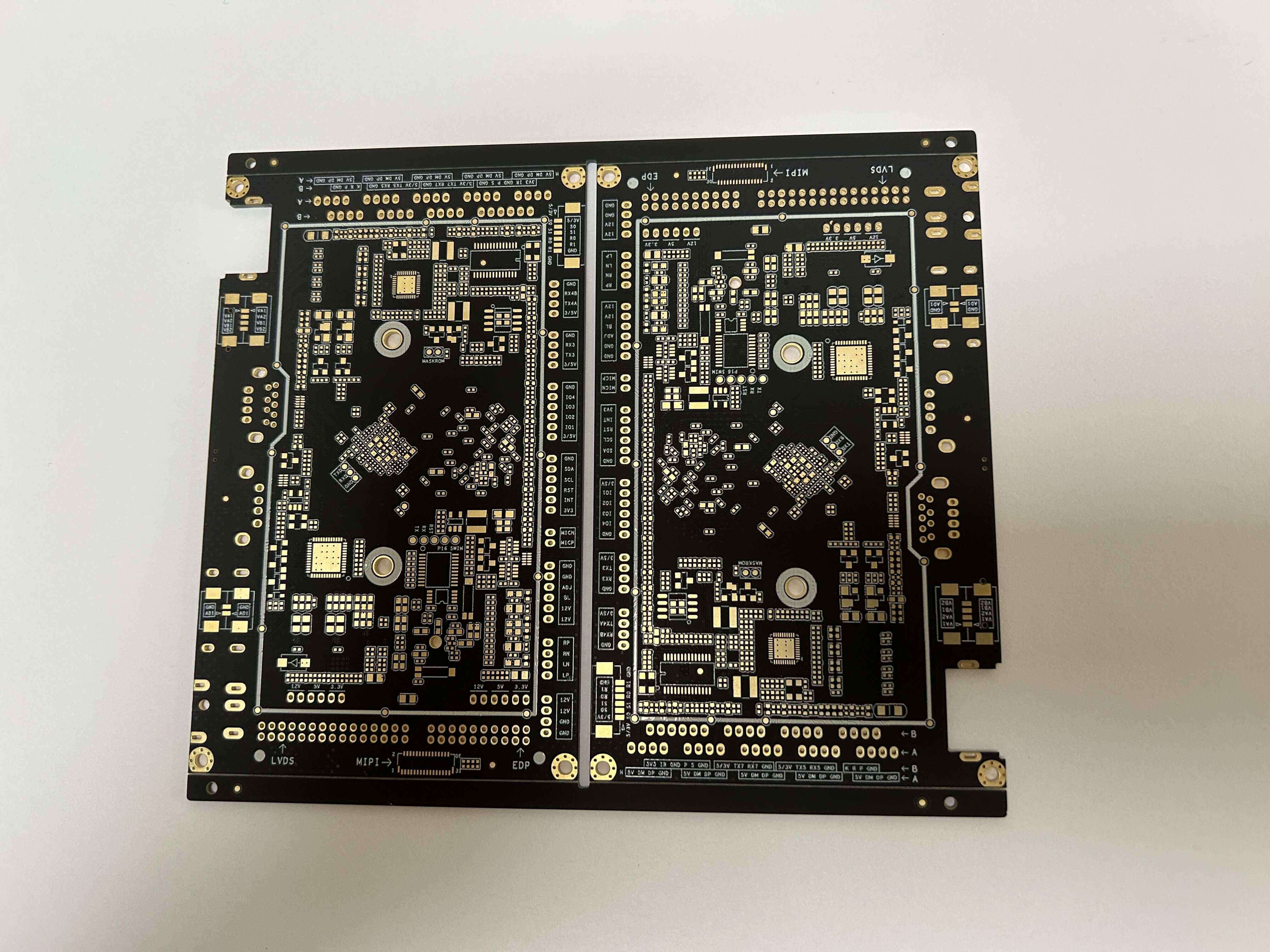
Multilayer PCBs are complex circuit boards that consist of multiple layers of conductive and insulating materials stacked together. These boards are commonly used in electronic devices due to their ability to accommodate more components in a smaller space while providing enhanced performance.
Benefits of Multilayer PCBs
Multilayer PCBs offer numerous advantages, including increased signal integrity, reduced electromagnetic interference, and improved thermal management. These benefits make them ideal for high-speed and high-frequency applications where performance and reliability are critical.
Design Considerations
When designing a multilayer PCB, it is essential to consider various factors such as layer stackup, signal routing, power distribution, and impedance control. Careful planning and attention to detail are crucial to ensure the functionality and reliability of the final product.
Best Practices for Multilayer PCB Design
To achieve success in multilayer PCB design, it is important to follow best practices such as using proper design tools, maintaining signal integrity, minimizing electromagnetic interference, and optimizing thermal performance. By adhering to these guidelines, designers can create robust and efficient multilayer PCBs.
Challenges and Solutions
Despite the many benefits of multilayer PCBs, designers may encounter challenges such as signal crosstalk, power integrity issues, and manufacturing complexities. However, by implementing advanced design techniques, utilizing simulation tools, and collaborating closely with manufacturers, these challenges can be overcome effectively.
Conclusion
In conclusion, multilayer PCB design is a complex yet rewarding process that requires a thorough understanding of circuit board fundamentals, design principles, and best practices. By mastering the intricacies of multilayer PCBs, designers can create innovative and reliable electronic devices that meet the demands of today's technology-driven world.


