1. Introduction
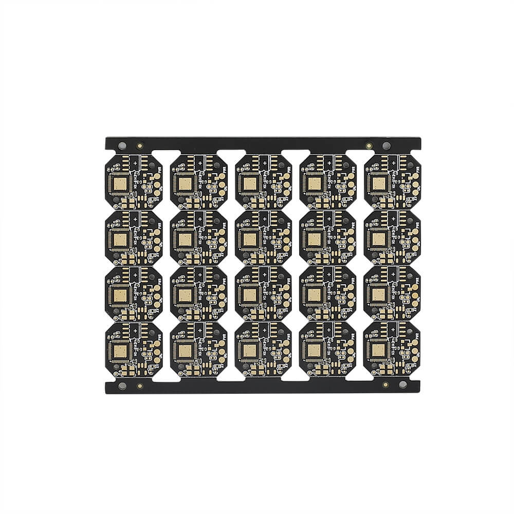
Double-sided PCB (Printed Circuit Board) is an electronic component substrate with the ability to lay out circuits along both sides of the board. It is made of conductive materials and has many important features to meet the needs of high-speed transmission and high-density component layout in complex electronic devices.
2. Structure and design
Double-sided PCBs consist of two conductive layers separated by an insulating layer (usually fiberglass-reinforced epoxy). The conductive layers are connected through holes (called vias), and electroplating methods are used to create good conductivity. Conductive layers on each side can be used to lay out circuit components and connection paths, allowing the transmission and control of electronic signals.
3. Advantages
Double-sided PCB has the following characteristics compared to single-sided PCB:
a) Higher component density: Double-sided PCB allows electronic components to be arranged on both sides, thus achieving higher component density than single-sided PCB.
b) Higher connectivity: Since double-sided PCB has multiple conductive layers and through-holes, the connection between circuit components is more flexible and reliable.
c) Better transmission performance: Double-sided PCB has better electrical performance and anti-interference ability in signal transmission, and can meet the requirements of high-speed signal transmission.
4. Applicable fields
Double-sided PCB is widely used in various types of electronic equipment, especially in the following fields:
a) Communication equipment: Double-sided PCB can be used in communication equipment such as mobile phones, wireless routers, base stations, etc. to achieve high-speed signal transmission and complex circuit layout.
b) Computer hardware: Double-sided PCB can be used for computer motherboards, graphics cards, embedded systems, etc. to meet high-speed data transmission and component density requirements.
c) Consumer electronics: Double-sided PCBs are widely used in consumer electronics products such as televisions, stereos, and game consoles to achieve multi-function and high performance.
5. Manufacturing difficulty and cost
Compared with single-sided PCB, double-sided PCB is more difficult and costly to manufacture. Since circuits need to be arranged on both sides, the conductive layers need to be positioned, connected and tested during the manufacturing process, making the manufacturing process more complex. At the same time, materials and processes such as insulation layers and through holes required for double-sided PCBs will also increase manufacturing costs.
To sum up, double-sided PCB has higher component density, connectivity and transmission performance, and is widely used in communication equipment, computer hardware, consumer electronics and other fields. However, the manufacturing difficulty and cost are relatively high. When choosing a PCB type, it is crucial to select the appropriate PCB type and manufacturer based on actual needs and budget considerations.

