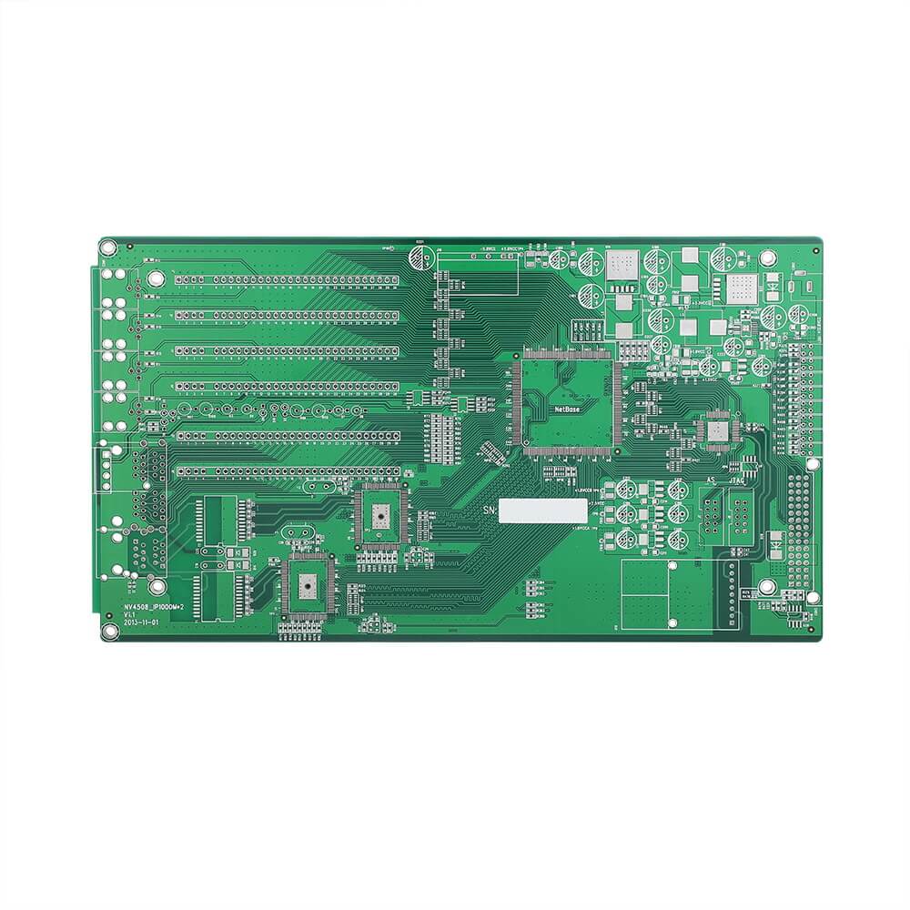
Overview of PCB double-sided manufacturing process
PCB (Printed Circuit Board) is a basic component widely used in modern electronic equipment. Among them, double-sided PCB is a common type of PCB, which has the characteristics of circuit lines on both sides. This article will introduce in detail the manufacturing process of PCB double-sided panels, including multiple steps such as design, printing, drilling, electroplating, depaneling and assembly.

1. Design stage
Before manufacturing a double-sided PCB, PCB design first needs to be done. Designers use professional PCB design software to create circuit diagrams and determine the size, layering and wiring rules of the board. The design phase also includes placing components and routing signal lines. As the design is completed, the design files are exported and used in subsequent manufacturing steps.
2. Printing and exposure
Printing is one of the key steps in PCB manufacturing. During the printing process, manufacturers transfer the design files to a copper-covered substrate. This is usually done by printing the design file onto a special photographic film, which is then placed over a copper-covered board. Next, the photo film is cured by exposure to light to preserve the circuit pattern. Finally, the uncovered copper film is removed through chemical etching to form a circuit pattern.
3. Drilling
Drilling is used to create holes in the printed board so that components can be inserted and connected. By using a CNC (Computer Numerical Control) drilling machine, manufacturers can drill holes according to design requirements. Drilling holes are usually used to connect the circuit lines of double-sided panels to achieve the transmission of signals and power.
4. Electroplating
By adding metal coverings to drilled holes and circuit lines, you can increase conductivity and enhance connection strength. Manufacturers immerse double-sided panels in a plating bath, using an electric current to deposit metal in the holes and on the copper. This process is called electroplating, and common metal materials include silver, nickel, and tin.
5. Disassembly and assembly
During the depaneling process, manufacturers cut large PCB boards containing multiple double-sided panels into individual panels. This is usually done using a hacksaw or other cutting tool. Once depaneling is complete, next comes the assembly phase. The manufacturer will solder the components onto the board and perform various tests to ensure the functionality and quality of the circuit.
In conclusion
The PCB double-sided manufacturing process is a complex but critical process that requires precise operation and strict control of multiple steps. From design to subboarding and assembly, every link requires strict quality control and professional technical support. Only in this way can the reliability and performance of double-sided PCBs be ensured.

