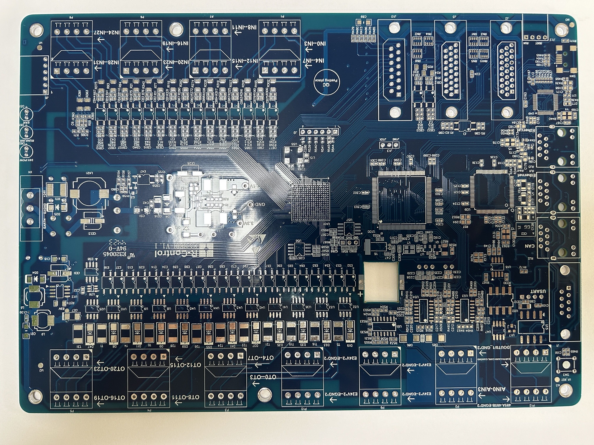
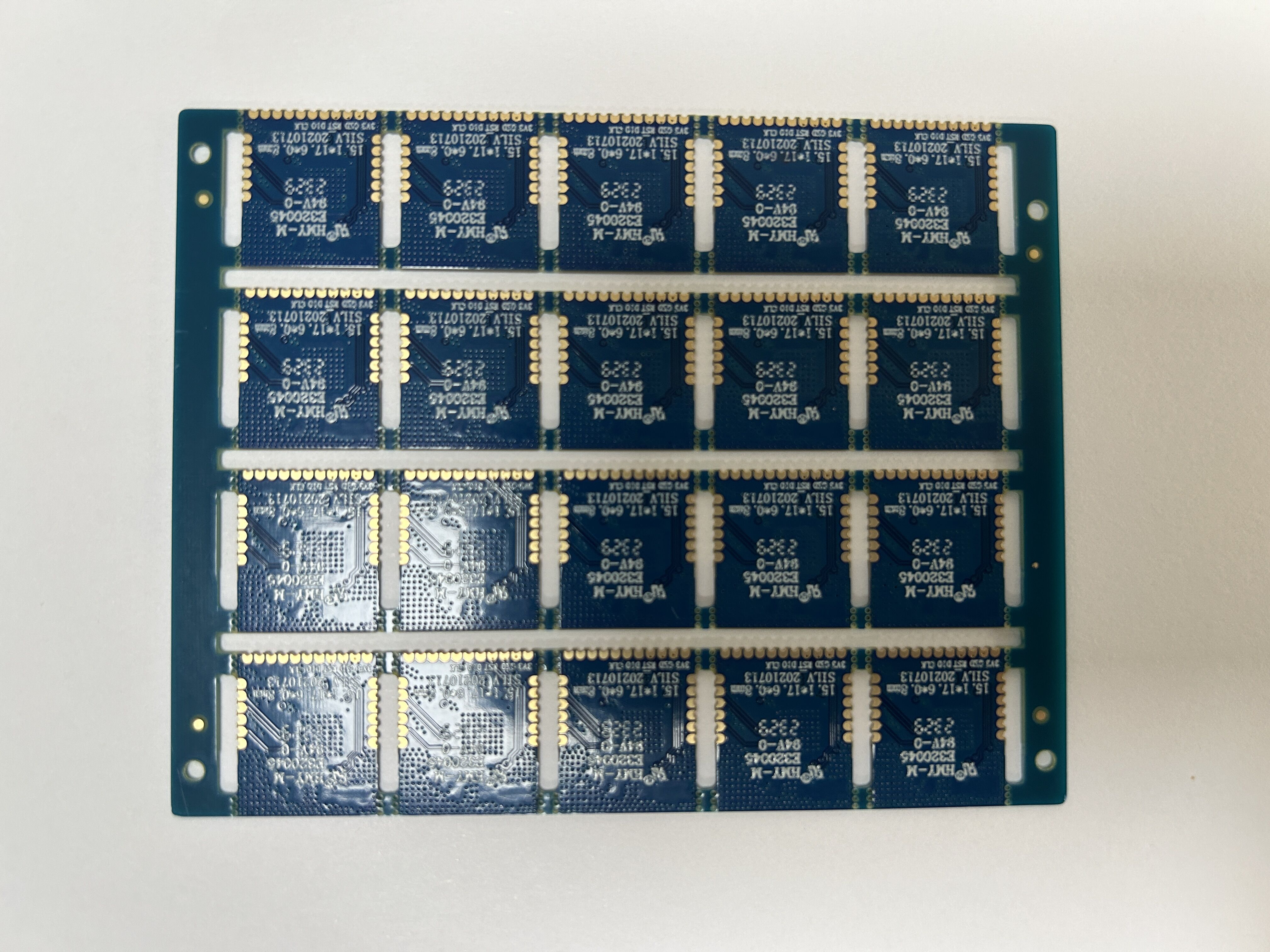
As technology advances, electronic devices demand faster signal processing and higher capacity, leading to the widespread adoption of High-Density Interconnect (HDI) technology in printed circuit boards (PCBs). As a professional HDI PCB manufacturer, Hongmy PCB is dedicated to delivering high-performance PCB solutions. At the same time, JLCPCB, a recognized leader in the PCB industry, has made significant contributions to advancing the sector. This article explores the types, advantages, disadvantages, and applications of HDI PCBs.
What is an HDI PCB?
HDI PCB, or High-Density Interconnect Printed Circuit Board, is a type of PCB with a higher wiring density. By incorporating microvias, fine lines, and high-performance materials, HDI PCBs allow for compact and efficient circuit designs. Compared to traditional PCBs, HDI PCBs accommodate more components in a smaller area, enabling the miniaturization and enhanced performance of electronic products.
At Hongmy PCB, we leverage state-of-the-art technology to produce top-quality HDI PCBs, advancing the industry alongside leading companies like JLCPCB.

Types of HDI PCBs
1.Standard HDI PCBs
Features microvias, blind vias, and buried vias for high-density interconnects.
Widely used in communication devices and consumer electronics for complex routing and high-speed signal transmission.
2.Stacked HDI PCBs
Built through a layer-by-layer lamination process, offering exceptional flexibility.
Ideal for compact, high-performance devices like smartphones and tablets.
3.Laser-Drilled HDI PCBs
Utilizes laser drilling to create precise microvias, suited for high-frequency and high-speed applications.
Commonly employed in digital communication and signal processing equipment.
4.Embedded Component HDI PCBs
Integrates components directly into the PCB layers, reducing device size while enhancing functionality.
At Hongmy PCB, we provide tailored solutions using these HDI technologies to meet diverse customer needs across various applications.
Advantages of HDI PCBs
1.Miniaturization and High Density
Compact Design: Allows more components to be mounted on both sides, reducing overall size.
High Component Density: Enables greater integration within limited space.
2.Improved Performance
Shorter Signal Paths: Shorter distances between components improve signal speed and minimize loss.
Better Signal Integrity: Reduces issues like signal reflection and electromagnetic interference.
Higher Frequencies: Supports faster signal processing and higher operating frequencies.
3.Enhanced Design Flexibility
Incorporates microvias, blind vias, and buried vias for more versatile designs.
Accommodates complex multi-layered structures.
4.Higher Reliability
Optimized Thermal Management: Improved heat dissipation and reduced thermal stress.
Reduced Parasitic Effects: Microvias lower parasitic inductance and capacitance.
5.Advanced Application Support
Compatible with modern technologies, including IoT devices, 5G networks, and advanced computing systems.

Disadvantages of HDI PCBs
1.Higher Manufacturing Costs
The use of specialized equipment (e.g., laser drilling machines) and processes increases production costs.
2.Complex Design Requirements
Requires sophisticated design tools and experienced engineers for precise layouts.
3.Assembly and Testing Challenges
High-density layouts and miniaturized components demand advanced assembly techniques and testing equipment like X-ray inspection.
4.Thermal Management Concerns
While thermal performance is improved, managing heat in high-power applications can remain a challenge.
Applications of HDI PCBs
Consumer Electronics
Smartphones and Tablets: Enable compact designs with enhanced performance.
Laptops: Meet lightweight design requirements while optimizing motherboard functionality.
Medical Devices
Diagnostic Equipment: Support precision diagnostics in devices like MRI and CT scanners.
Portable Devices: Enhance stability in compact devices such as blood pressure monitors and glucometers.
Telecommunications
Routers and Transmitters: Ensure compact designs with high-speed data transfer.
5G Base Stations: Support high-performance and dense circuitry demands of 5G networks.
Automotive Industry
Advanced Driver Assistance Systems (ADAS): Used in radar, cameras, and sensors.
Electric Vehicles: Play a critical role in battery management systems and power conversion devices.
Hongmy PCB serves these diverse industries by delivering reliable and high-performance HDI PCB solutions. By drawing inspiration from companies like JLCPCB, we continuously improve our manufacturing processes to create value for our customers.

At Hongmy PCB, we remain committed to providing advanced HDI technology to meet the growing demands of modern electronics. From consumer electronics and medical devices to telecommunications and automotive systems, HDI PCBs demonstrate immense potential across various applications.
For more information about our HDI PCB solutions or to discuss your specific requirements, please contact Hongmy PCB today.

