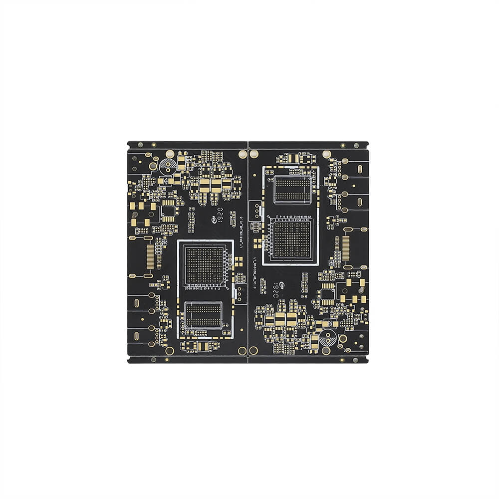
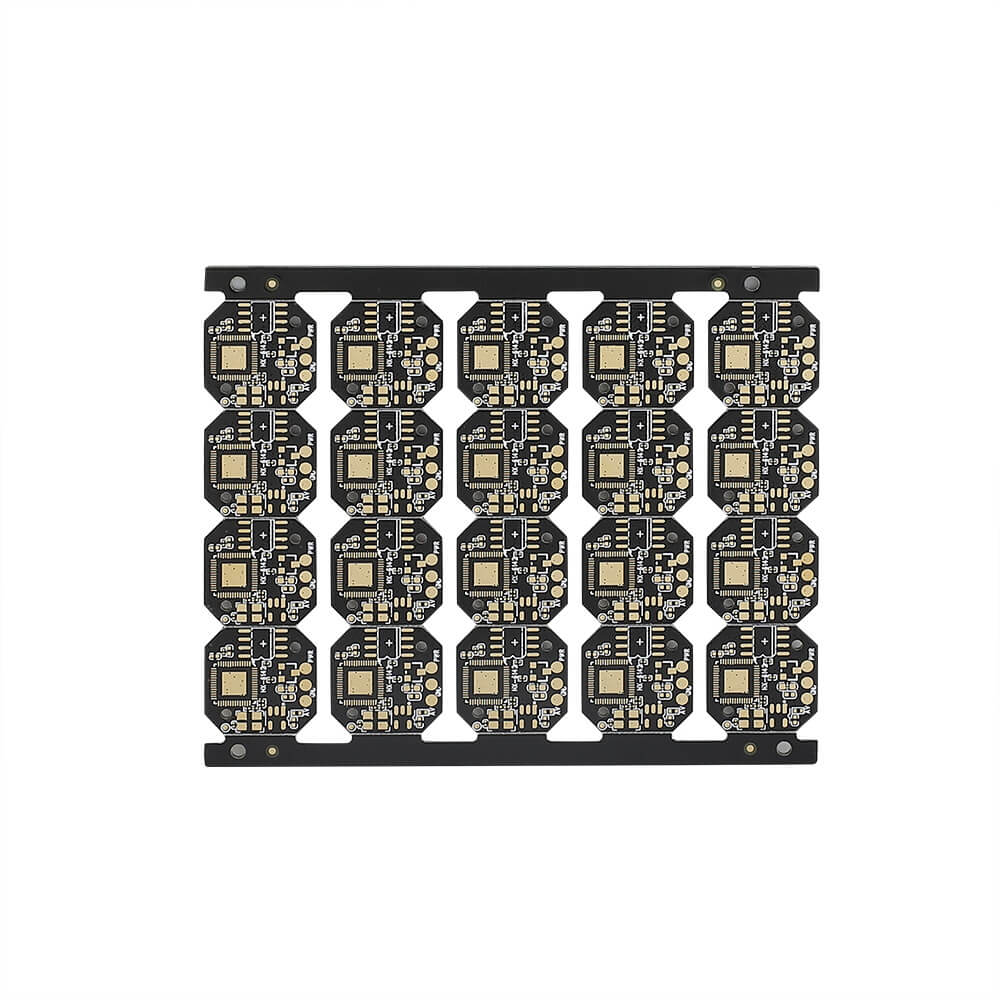
Printed Circuit Boards (PCBs) are fundamental to modern electronics, providing the platform for electrical connections in a wide array of devices. The complexity and capabilities of PCBs vary widely, with single-sided and double-sided pcbs being among the most common types. Understanding the differences in their manufacturing processes is crucial for selecting the right PCB type for specific applications.
Single-Sided PCBs: Simplicity and Efficiency
1. Basic Structure:
Single-sided PCBs have only one layer of conductive material (typically copper) on one side of the board. The other side is left as a substrate, usually made of materials like FR-4 (a fiberglass-reinforced epoxy laminate).
2. Manufacturing Steps:
Material Preparation:
The manufacturing process begins with a base substrate, commonly FR-4, which is laminated with a copper foil.
Design Transfer:
A photoresist layer is applied to the copper surface. The board is then exposed to UV light through a mask that outlines the circuit design. The exposed photoresist hardens, while the unexposed areas remain soft and are washed away.
Etching:
The board undergoes a chemical etching process where the exposed copper is removed, leaving only the copper traces protected by the hardened photoresist.
Drilling:
Any necessary holes for component leads or vias are drilled.
Solder Mask and Silkscreen:
A solder mask is applied to protect the copper traces and prevent solder bridges during component soldering. A silkscreen layer is added to print component labels and other markings.
Component Assembly:
Components are soldered onto the board, either manually or through automated soldering techniques like wave soldering.

Advantages of Single-Sided PCBs:
Simplicity in design and manufacturing.
Lower cost compared to multi-layer PCBs.
Suitable for low-density, low-complexity applications.
Double-Sided PCBs: Enhanced Connectivity and Complexity
1. Basic Structure:
Double-sided PCBs have conductive layers on both sides of the board. This allows for more complex circuits and higher component density compared to single-sided PCBs.
2. Manufacturing Steps:
Material Preparation:
Similar to single-sided PCBs, double-sided PCBs start with a substrate material like FR-4, laminated with copper on both sides.
Design Transfer:
Both sides of the board are coated with photoresist and exposed to UV light through masks that outline the circuit design for each side. This step requires precise alignment to ensure that the vias (holes that connect traces on different layers) are correctly positioned.
Etching:
The board undergoes chemical etching to remove unprotected copper from both sides, creating the required circuit patterns.
Drilling:
Holes are drilled through the board to create vias that connect traces on the top and bottom layers.
Plating:
The drilled holes are plated with copper to form electrical connections between the top and bottom layers. This step, called through-hole plating, is crucial for the functionality of double-sided PCBs.
Solder Mask and Silkscreen:
A solder mask is applied to both sides of the board to protect the copper traces and prevent solder bridges. Silkscreen layers are added to both sides for component labeling and other markings.
Component Assembly:
Components can be mounted on both sides of the board, increasing the board's complexity and functionality. This step may involve surface mount technology (SMT) or through-hole technology (THT), depending on the components used.
Advantages of Double-Sided PCBs:
Greater circuit density and complexity.
Ability to accommodate more components and connections.
Enhanced functionality for more advanced applications.

Key Differences in Manufacturing Processes
1. Material Use:
Single-sided PCBs use a single layer of copper, while double-sided PCBs use copper layers on both sides.
2. Design Transfer and Etching:
Single-sided PCBs involve a simpler design transfer process, as only one side needs patterning and etching. Double-sided PCBs require precise alignment and patterning on both sides.
3. Drilling and Plating:
Single-sided PCBs may have simple through-holes for component leads. In contrast, double-sided PCBs require through-hole plating to electrically connect the two sides of the board.
4. Complexity and Functionality:
Double-sided PCBs allow for more complex designs and higher component density, making them suitable for advanced applications.
Conclusion
The choice between single-sided and double-sided PCBs depends on the complexity and requirements of the application. Single-sided PCBs are cost-effective and simpler to manufacture, making them ideal for straightforward, low-density circuits. Double-sided PCBs, with their ability to accommodate more complex and dense circuits, are essential for more advanced electronic devices. Understanding these differences helps in selecting the right type of PCB for your project, ensuring optimal performance and cost-efficiency.

