

High-Quality HDI PCB HDI Circuit Board Manufacturer China
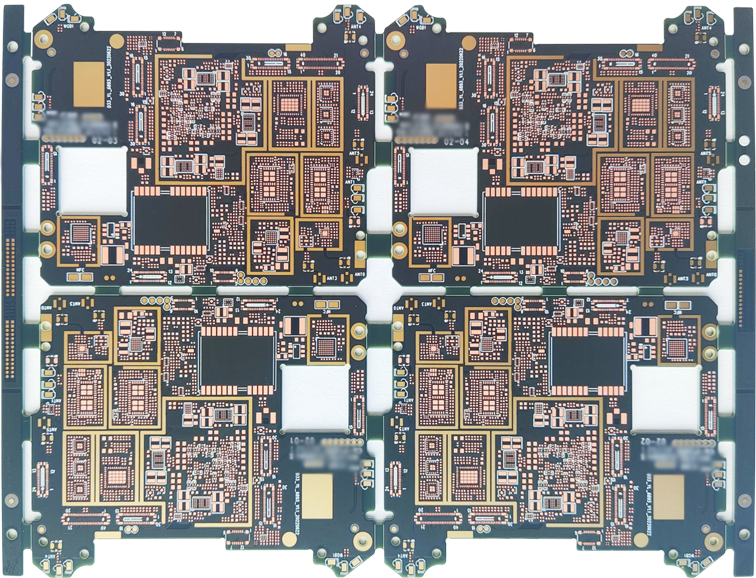
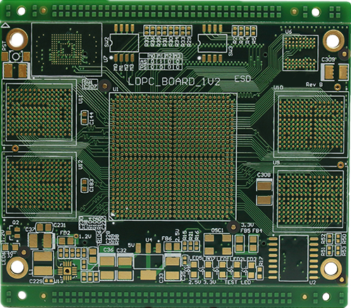
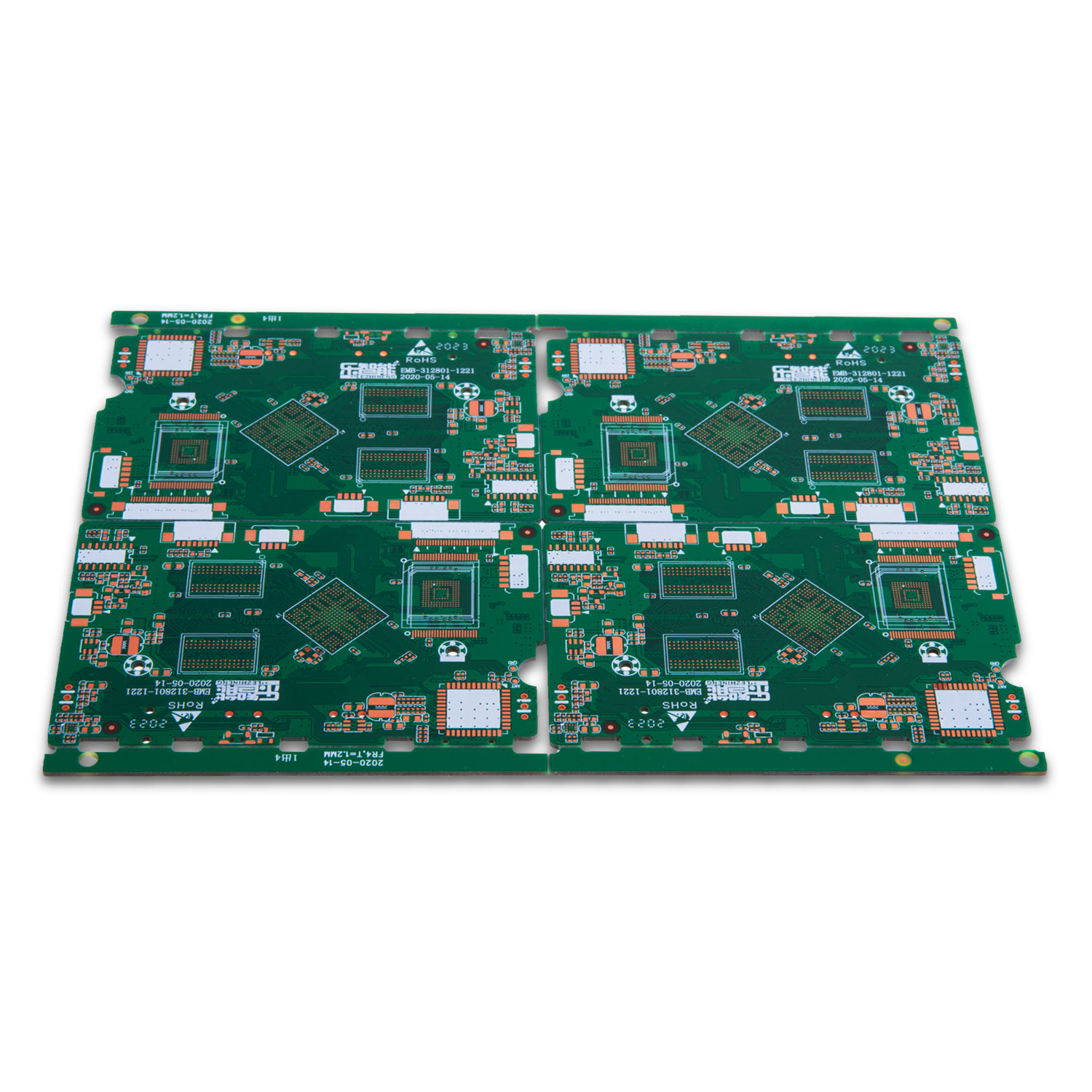
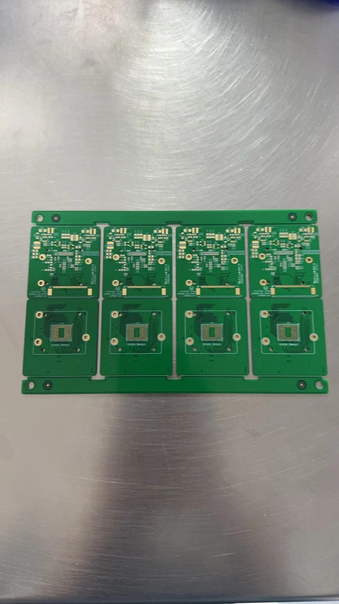
Product description
Product parameters
Item NO.: Hongmy –HM106
Layer: 10layers
HDI:1+N+1
Material: FR4
Finished Board Thickness: 1.6MM
Finished Copper Thickness: 1OZ
Min Line Width/Space: ≥3mil(0.075mm)
Min Hole: ≥4mil(0.1mm)
Surface Finish: ENIG
Solder Mask Color: Green
Legend Color: White
Application: Airplane Model/Intelligent Home Appliance/Smart Watch/BMS /ATC
")
Common Buildup Structure
The difference between HDI PCB and ordinary PCB, you can see from the Buildup Structure.
The Stackup show 1+ N +1 and 2+N+2 HDI PCB Structure
")
HDI boards typically feature:
- Microvias: Smaller vias than in traditional PCBs, enabling compact designs.
- Blind and buried vias: These vias connect different layers of the PCB without passing through the entire board, optimizing space.
- Built-up laminations: Multiple layers of laminates are built up to increase functionality in a compact design.
- High signal performance: As these boards support faster signal transmission, they are ideal for high-speed applications.
HDI boards, compared to traditional PCBs, are smaller, lighter, and can replace multiple PCBs by integrating more functions into a single board. This results in lower layer counts and more compact designs. The standards governing HDI design and fabrication include IPC-2315, IPC-2226, IPC-4104, and IPC-6016.
The advantages of HDI PCB
HDI (High-Density Interconnect) PCBs offer several key advantages over traditional PCBs, making them an increasingly popular choice in modern electronic design and manufacturing. Below are the primary benefits of HDI PCB technology:
- Cost Reduction: HDI PCBs can reduce overall production costs, especially for complex designs with more than 8 layers. With optimized designs, fewer layers and boards are required, minimizing material and manufacturing expenses.
- Improved Electrical Performance: HDI PCBs offer better signal accuracy and performance due to shorter distances between components and traces. This improves signal integrity, reduces power consumption, and supports high-speed electronics.
- Enhanced Thermal Properties: HDI technology allows for better heat dissipation, improving the overall thermal performance of the PCB. This is essential for applications where overheating can be an issue.
- Reduced Electromagnetic Interference: HDI boards are designed to minimize radio frequency interference (RFI), electromagnetic wave interference (EMI), and electrostatic discharge (ESD). This leads to more stable and reliable electronic devices, particularly in sensitive environments.
- Smaller, More Compact Designs: HDI allows for the placement of more components on both sides of the PCB and uses advanced via processes (like blind and buried vias), freeing up more space for component placement. This enables the production of smaller, lighter, and more compact devices without sacrificing functionality.
- Faster Signal Transmission: By shortening the distance between components and reducing the size of the vias, HDI PCBs ensure faster signal transmission with minimal signal loss or delay, making them ideal for high-speed, high-frequency applications.
- Greater Reliability: Microvias in HDI PCBs are more reliable than traditional through-hole vias due to their smaller aspect ratio. This results in better performance, durability, and long-term reliability.
- Faster Time-to-Market: The optimized design and manufacturing process of HDI PCBs reduce the time required for production, design, and testing, helping businesses get their products to market faster.
HDI PCBs are ideal for applications where space, performance, and reliability are critical, such as in consumer electronics, telecommunications, and automotive industries. With the ability to “do more with less,” they are a powerful solution for modern electronic devices.
Design Guide
Limited Board Workspace: HDI PCB designs typically face constraints in available workspace, requiring efficient use of every inch of the board.
Smaller Components and Tighter Spacing: As components get smaller, HDI PCBs require precise routing and layout to ensure sufficient spacing between elements.
More Components on Both Sides of the PCB: HDI technology allows for more components to be placed on both sides of the PCB, increasing design flexibility and functionality.
- Longer Trace Routes Leading to Extended Signal Flight Times: The increased trace lengths between components may result in longer signal transmission times.
- More Trace Routes Needed: As design complexity increases, more trace routes are typically required to complete the board’s circuit connections.
- Trace Width and Spacing Limits: In high-density designs, trace width and spacing are limited and must adhere to strict design rules and manufacturing capabilities.
- Annular Ring and Aspect Ratio Limits: Especially in high-reliability designs, there are limitations on annular rings and aspect ratios, affecting via design.
- Material System for Controlled Impedance: The material system used in the PCB must support controlled impedance, which is critical for maintaining signal integrity.
- Impedance Profiles for Desired Stackup: If available, impedance profiles must be considered when selecting the appropriate stackup or layer pairs to meet performance requirements.
Material Characteristics of HDI PCB
")
")
")