

HDI PCB Fabrication Sourcing Ro4003 Ro4350B Immersion Gold China Factory
Product description
Product parameters
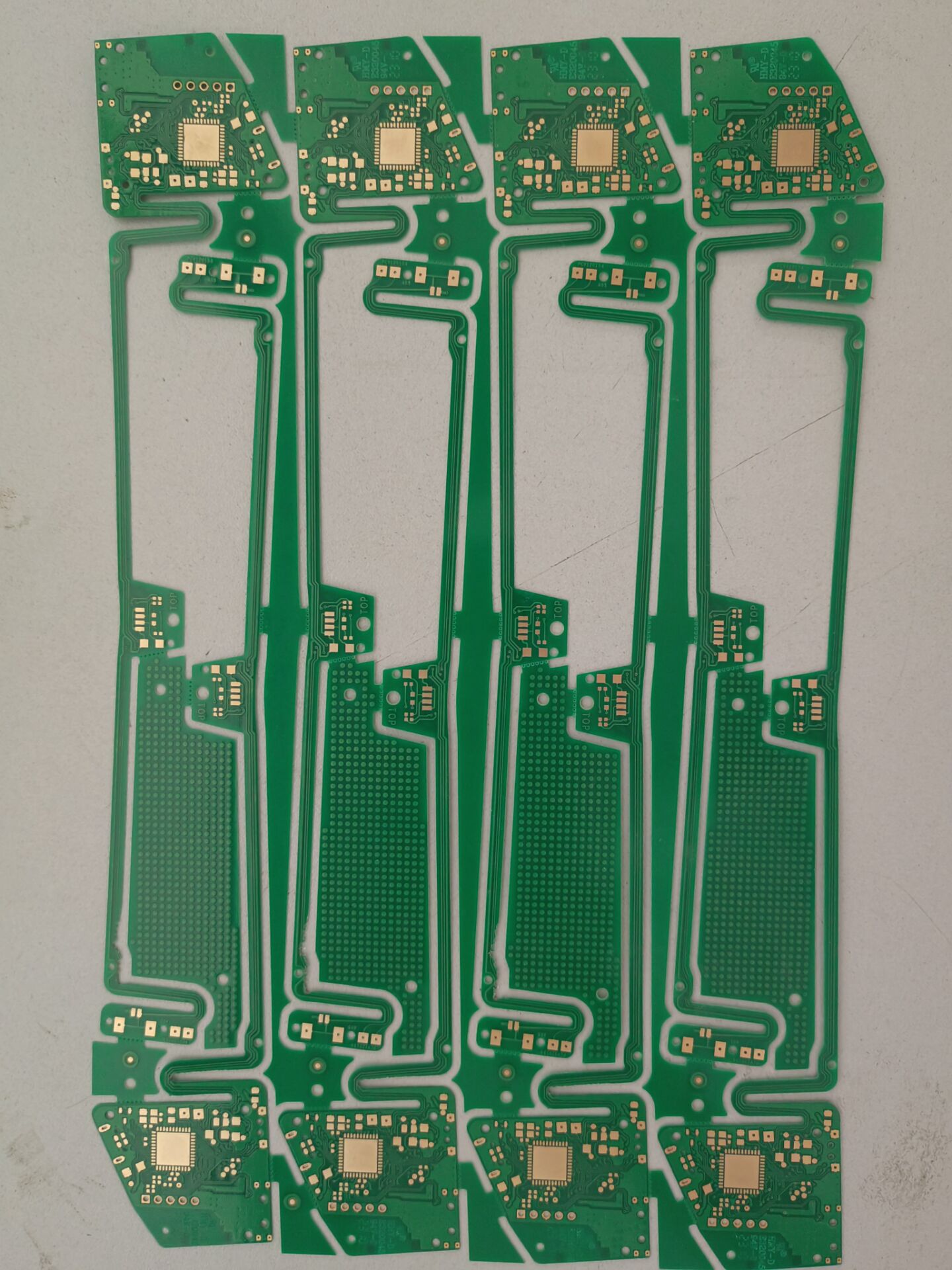
Item NO.: Hongmy –HM041
Layer: 12layers
HDI:2+N+2
Material: FR4(SH260)
Finished Board Thickness: 1.6MM
Finished Copper Thickness: 1OZ
Min Line Width/Space: ≥3mil(0.075mm)
Min Hole: ≥4mil(0.1mm)
Surface Finish: ENIG
Solder Mask Color: Green
Legend Color: White
Application: Intelligent Home Appliance/Smart Watch/Bluetooth Speakers
")
FR4 PCB Introduction
--Definition
FR means “flame-retardant,” FR-4 (or FR4) is a NEMA grade designation for glass-reinforced epoxy laminate material, a composite material composed of woven fiberglass cloth with an epoxy resin binder that makes it an ideal substrate for electronic components on a printed circuit board.
")
-Pros and Cons of FR4 PCB
FR-4 material is so popular because of its many wondrous qualities that can benefit printed circuit boards. In addition to being affordable and easy to work with, it is an electrical insulator with very high dielectric strength. Plus, it's durable, moisture-resistant, temperature-resistant and lightweight.
FR-4 is a widely relevant material, popular mostly for its low cost and relative mechanical and electrical stability. While this material features extensive benefits and is available in a variety of thicknesses and sizes, it isn't the best choice for every application, especially high-frequency applications like RF and microwave designs.
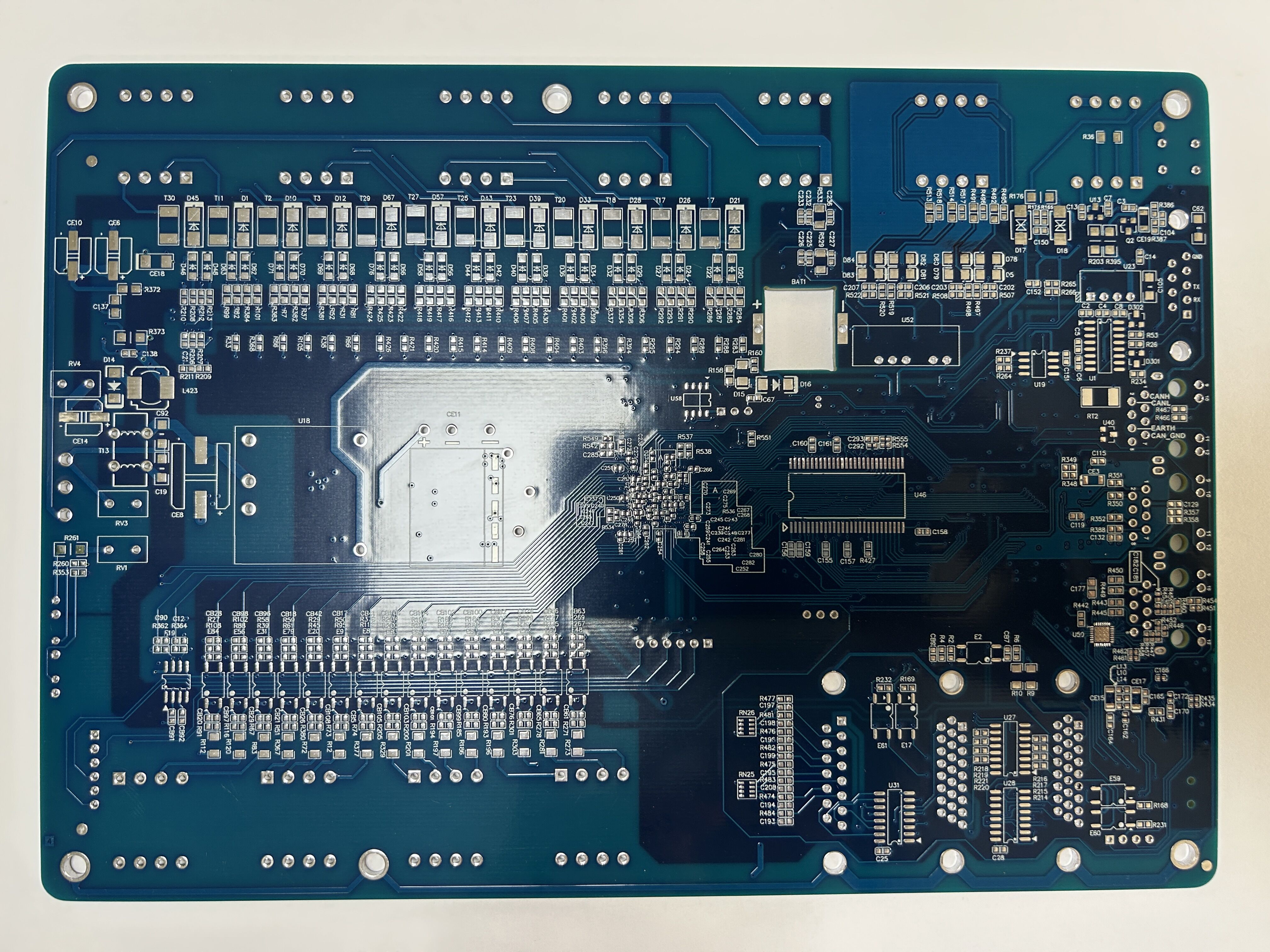
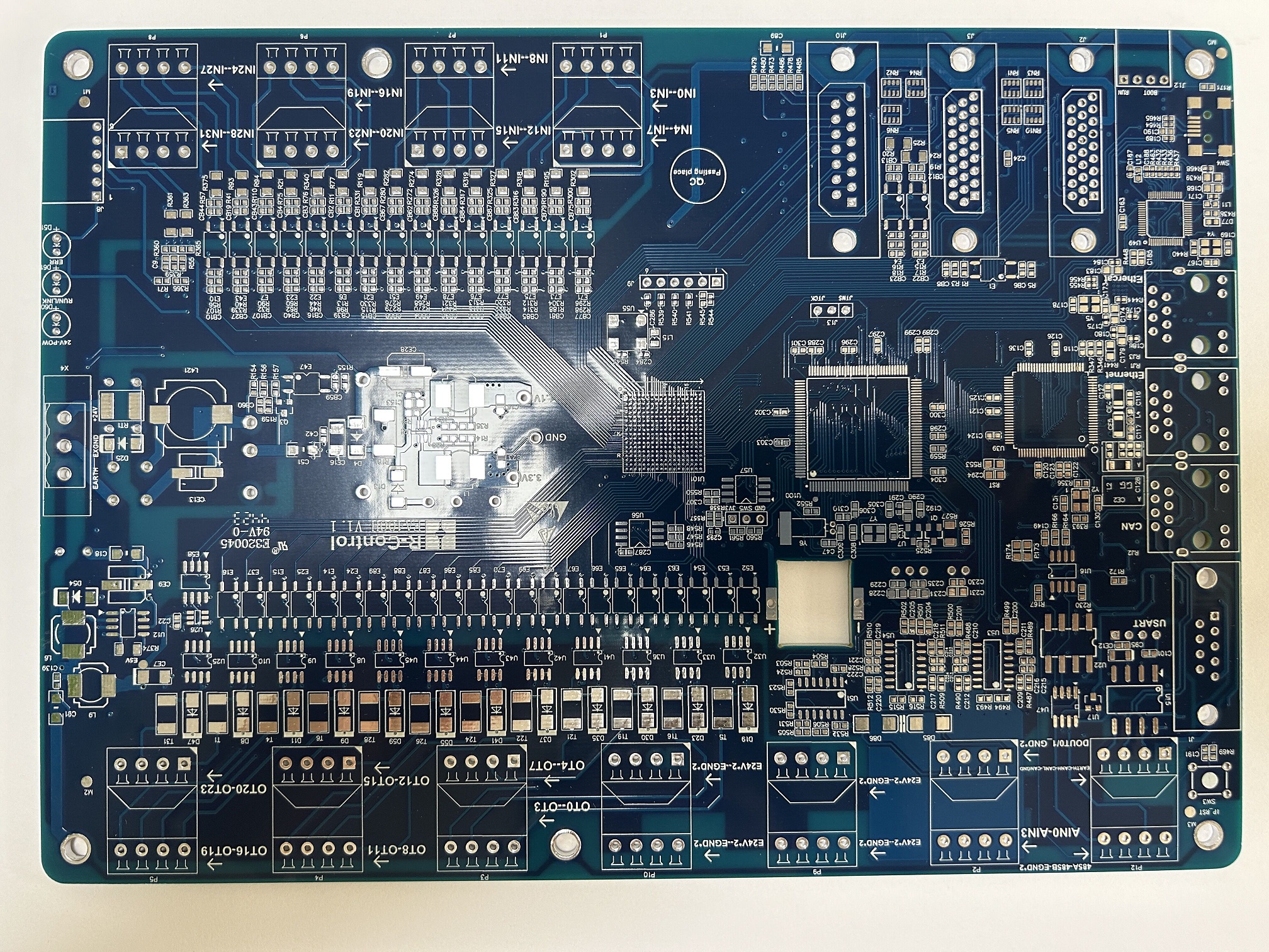
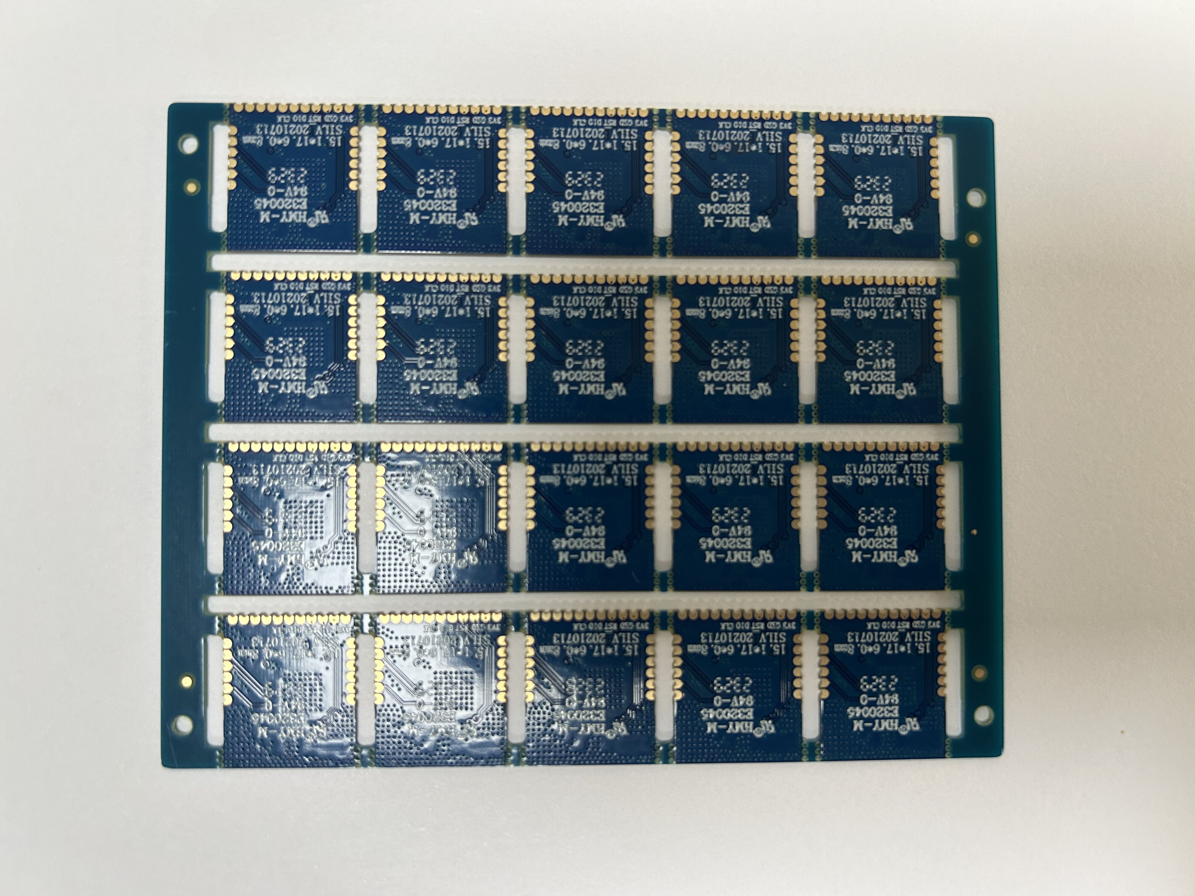
-Multi-layer PCB Structure
Multilayer PCBs further increases the complexity and density of PCB designs by adding additional layers beyond the top and bottom layers seen in double sided boards. Multilayer PCBs are built by laminating the various layers. The inner-layers, normally double-sided circuit boards, are stacked together, with insulating layers in between and between the copper-foil for the outer-layers. Holes drilled through the board (vias) will make connections with the different layers of the board.
Definition
HDI: High-Density Interconnect. There are many different definitions of HDI technology. Common for all HDI boards is the use of smaller trace & space and microvias to create higher wiring routing density than a conventional PCB.Increased circuit density and complexity.More complex designs can be adopted, potentially allowing different single sided and/or double sided designs to be incorporated into one multilayer design.Reduction in size due to extra routing space from additional layers.Improved distribution of power, better ground shielding and good return paths for signals.Segregation of critical design aspects e.g. digital and analogue or high speed/high frequency.Better EMC compliance from use of ground or power plane layers.
Key HDI Benefits
As consumer demands change, so must technology. By using HDI technology, designers now have the option to place more components on both sides of the raw PCB. Multiple via processes, including via in pad and blind via technology, allow designers more PCB real estate to place components that are smaller even closer together. Decreased component size and pitch allow for more I/O in smaller geometries. This means faster transmission of signals and a significant reduction in signal loss and crossing delays.
Via in Pad Process
Inspiration from surface mount technologies from the late 1980's has pushed the limits with BGA's, COB and CSP into smaller square surface inches. The via in pad process allows for vias to be placed within the surface of the flat lands. The via is plated and filled with either conductive or non-conductive epoxy then capped and plated over, making it virtually invisible.
Sounds simple but there is an average of eight additional steps to complete this unique process. Specialty equipment and trained technicians follow the process closely to achieve the perfect hidden via.
Via Fill Types
There are many different types of via fill material: non conductive epoxy, conductive epoxy, copper filled, silver filled and electrochemical plating. These all result in a via buried within a flat land that will completely solders as normal lands. Vias and microvias are drilled, blind or buried, filled then plated and hidden beneath SMT lands. Processing vias of this type requires special equipment and is time consuming. The multiple drill cycles and controlled depth drilling adds to process time.
Cost Effective HDI
While some consumer products shrink down in size, quality remains the most important factor for the consumer second to price. Using HDI technology during design, it is possible to reduce an 8 layer through-hole PCB to a 4 layer HDI microvia technology packed PCB. The wiring capabilities of a well-designed HDI 4 layer PCB can achieve the same or better functions as that of a standard 8 layer PCB.
Although the microvia process increases the cost of the HDI PCB, the proper design and reduction in layer count reduces cost in material square inches and layer count more significantly.
Building Non-Conventional HDI Boards
Successful manufacturing of HDI PCBs requires special equipment and processes such as laser drills, plugging, laser direct imaging and sequential lamination cycles. HDI boards have thinner lines, tighter spacing and tighter annular ring, and use thinner specialty materials. In order to successfully produce this type of board, it requires additional time and a significant investment in manufacturing processes and equipment.
")
")
")