

PCB Factory of Multilayer PCB FR4 94V0 Printed Circuit Board
Product description
Product parameters
Item NO.: Hongmy –HM008
Layer: 4layer
Material: FR4
Finished Board Thickness: 2/1.6MM
Finished Copper Thickness: 1OZ
Min Line Width/Space: ≥3mil(0.075mm)
Min Hole: ≥4mil(0.1mm)
Surface Finish: HASL-LF
Solder Mask Color: Green
Legend Color: White
Application: Consumer Electronics
FR4 PCB Introduction
--Definition
FR means “flame-retardant,” FR-4 (or FR4) is a NEMA grade designation for glass-reinforced epoxy laminate material, a composite material composed of woven fiberglass cloth with an epoxy resin binder that makes it an ideal substrate for electronic components on a printed circuit board.
")
-Pros and Cons of FR4 PCB
FR-4 material is so popular because of its many wondrous qualities that can benefit printed circuit boards. In addition to being affordable and easy to work with, it is an electrical insulator with very high dielectric strength. Plus, it's durable, moisture-resistant, temperature-resistant and lightweight.
FR-4 is a widely relevant material, popular mostly for its low cost and relative mechanical and electrical stability. While this material features extensive benefits and is available in a variety of thicknesses and sizes, it isn't the best choice for every application, especially high-frequency applications like RF and microwave designs.
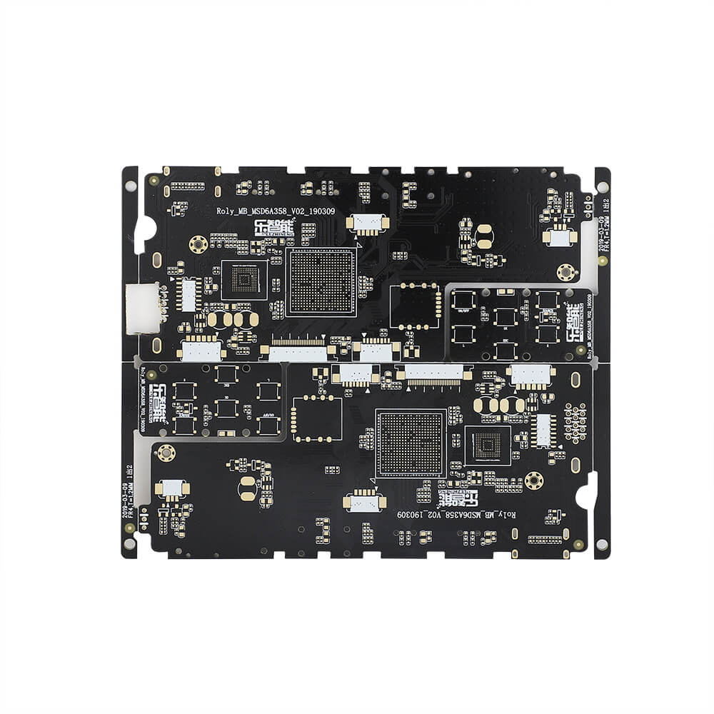
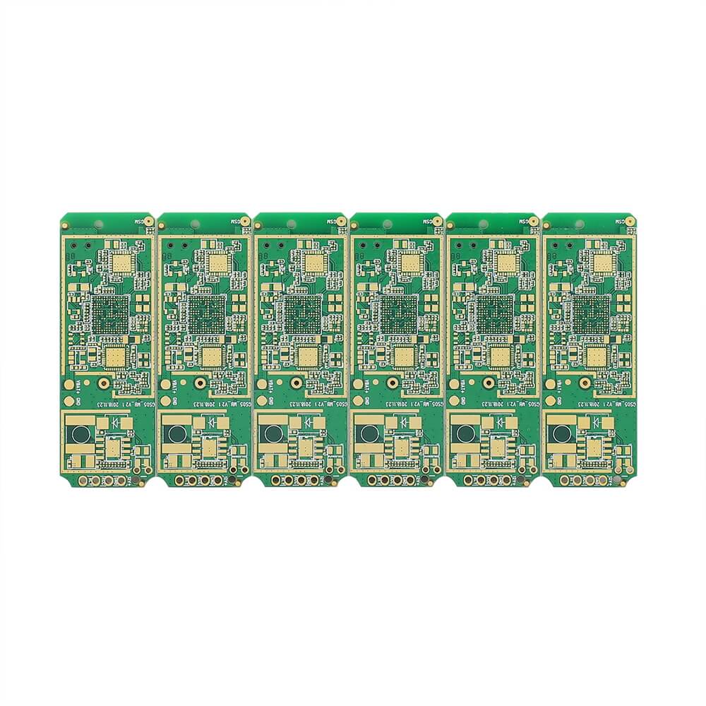
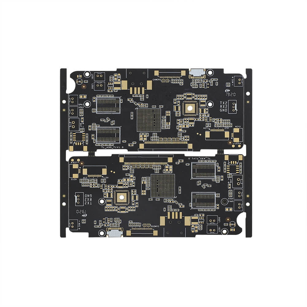
-Multi-layer PCB Structure
Multilayer PCBs further increases the complexity and density of PCB designs by adding additional layers beyond the top and bottom layers seen in double sided boards. Multilayer PCBs are built by laminating the various layers. The inner-layers, normally double-sided circuit boards, are stacked together, with insulating layers in between and between the copper-foil for the outer-layers. Holes drilled through the board (vias) will make connections with the different layers of the board.
Definition
HDI: High-Density Interconnect. There are many different definitions of HDI technology. Common for all HDI boards is the use of smaller trace & space and microvias to create higher wiring routing density than a conventional PCB.Increased circuit density and complexity.More complex designs can be adopted, potentially allowing different single sided and/or double sided designs to be incorporated into one multilayer design.Reduction in size due to extra routing space from additional layers.Improved distribution of power, better ground shielding and good return paths for signals.Segregation of critical design aspects e.g. digital and analogue or high speed/high frequency.Better EMC compliance from use of ground or power plane layers.
")
")
")
")